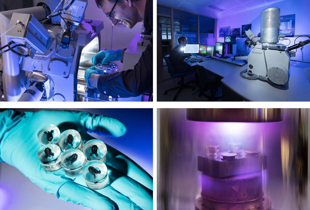
Scanning Electron Microscopy (SEM)
Contact person

The Scanning Electron Microscope (SEM) is a versatile instrument. Our microscope is a FEI Nova NanoSEM 650. The sample chamber is large, allowing samples up to 15 cm across to be inserted. The field of view is from about 1 mm down to a few hundred nm. Details down to a few tens of nm can be seen.
The SEM can handle electrically conductive or insulating materials e.g. metals, polymers, semiconductors, ceramics and electronics. There is also a dedicated transmission detector allowing the microscope to see thru thin samples. The EDS system attached is able to detect the presence of elements from Be to U in the periodic table without prior knowledge. The EBSD system attached can map the crystallography of the sample and identify the phases present.
Relevant links
Infrastructure networks:
Projects:
