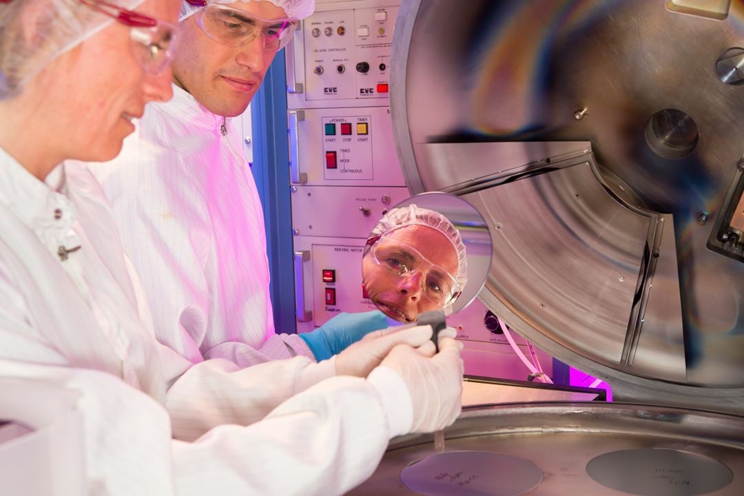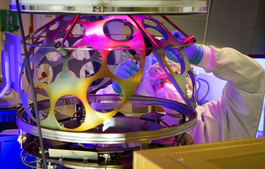
Our research includes activities aimed at increasing the efficiency and lowering the cost of solar cells. SINTEF has the equipment and expertise for deposition of thin films with a variety of methods, and for characterization of these structures.
Some examples of different activities are:
• Nanostructured Si / Al thin films deposited by magnetron sputtering: This creates three-dimensional silicon-based nanostructures, at room temperature and without the use of precursors, with interesting optoelectronic properties. There structures can increase the absorption of light in solar cells.
• Quantum dots of Si in SiO2 deposited by PE-CVD: The aim is to make structures that can make use of high-energy electromagnetic radiation in solar cells. The structures will enable radiation to be absorbed closer to the p-n junction in a Si solar cell. This can reduce the recombination of charge carriers and, thus, increase the efficiency of the solar cell.
• Black Silicon structures made using metal-catalysed etching: The aim of this activity is to structure the Si-surface in order to absorb as much of the incoming light as possible. The more light absorbed, the more electricity we get.
• Thinner and cheaper solar cells: The solar cells we have today can be made thinner, better and cheaper. The aim of this activity is to reduce material consumption and costs associated with the production of solar cells.

