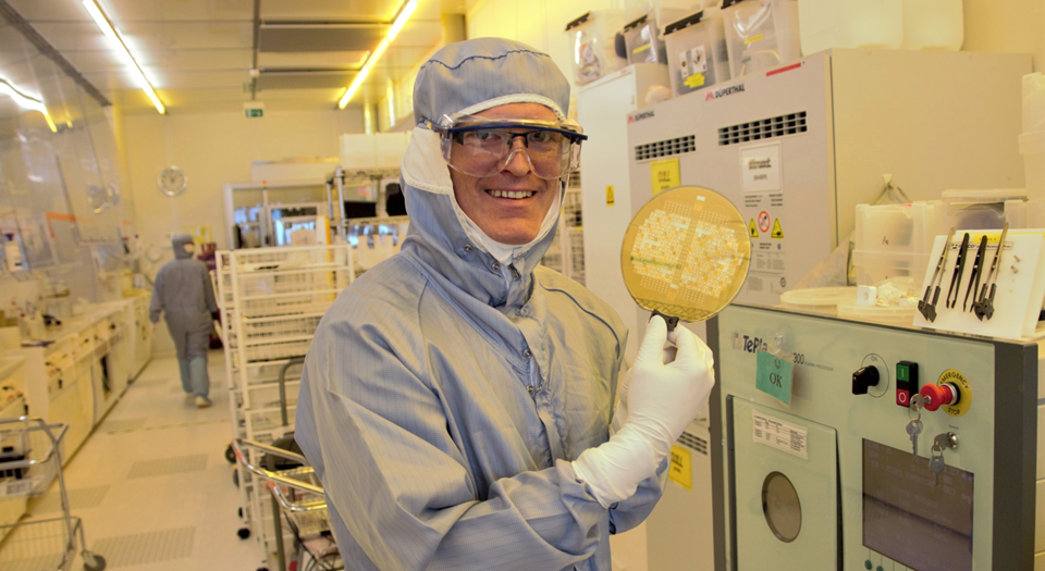
SINTEF researcher Frode Tyholdt’s face is reflected in the shiny surface of a wafer with piezoelectric material that was manufactured using a process that he himself has developed at the SINTEF MiNaLab. The abbreviation PiezoMEMS stands for Piezoelectric Micro-ElectroMechanical systems. SINTEF has been conducting research into this subject for almost twenty years, making Norwegian researchers world leaders in this field today.
The wafer can be used to make so-called MEMS chips with a wide range of high-tech applications. Just to mention a few, PiezoMEMS technology is used in super-fast cameras in mobile phones, and plays an important role in high-speed internet transmission. It provides machines with the ability to separate different kinds of plastics during waste recycling, and can be used to check water quality at our fish farms.
The Norwegian company poLight was one of the first to apply SINTEF’s technology in an autofocus camera lens for mobile phones.
“The advantage is that the lens uses little electricity and can change its shape in just a millisecond. This makes focusing lightning fast compared to other lenses”, says Tyholdt.
But how does piezoelectricity work?
Tyholdt explains:
A charge is induced across a piezoelectric crystal when it is deformed. In 1880, Jacques and Pierre Curie discovered the so-called piezoelectric effect (from the Greek piezein, meaning to “press” or “squeeze”) observed in some crystalline minerals. In such crystals, the atoms are not arranged entirely symmetrically. This means that the balance between the positive and negative charges (the atoms) is disrupted when the material is deformed, causing a net charge to be induced across the material.
Facts about piezoelectric materials:
Piezoelectric materials have been in use for many years. A traditional application is in ultrasound for medicine and underwater surveying (SONAR). Norwegian researchers are among the global elite when it comes to the development of piezoMEMS technology and SINTEF has patented many of the MEMS chips it has developed. SINTEF is currently working to develop the technology in-house at SINTEF MiNaLab by the Oslo Research Park, with funding from the EU and the Research Council of Norway, and in collaboration with its clients.
For more information: www.piezomems.com
This also works in the opposite direction. If we apply a voltage across a piezoelectric material, the atoms will move in response to electrostatic forces, causing the material to expand. This is the principle behind the components that we have developed at SINTEF.
Manufactured in an ultra-clean lab
Tyholdt struck gold during his doctorate studies at the University of Oslo. He developed a process to integrate silicon with piezoelectric PZT, a hard ceramic substance consisting of lead, zirconium, titanium and oxygen, which made it possible to manufacture piezoMEMS wafers.
Today, these wafers are manufactured in SINTEF’s cleanroom MiNaLab. It has to be so clean here that we have to wear “top-to-bottom” lab suits that make us look like Michelin men. In the most critical areas, not even so much as a grain of dust is permitted to enter the room, let alone a camera. But fortunately, the lab has its own.
Tyholdt’s colleague Jo Gjessing is in the lab, studying the wafer under a microscope. It will later be diced into MEMS chips, which are manufactured using half-millimetre thick silicon wafers that look a bit like large CDs, covered with a thin (100 nanometres) platinum electrode coating. On top of this is a piezoelectric film, consisting of a 1-2 micrometre-thick layer of PZT material (lead zirconium titanium oxide).
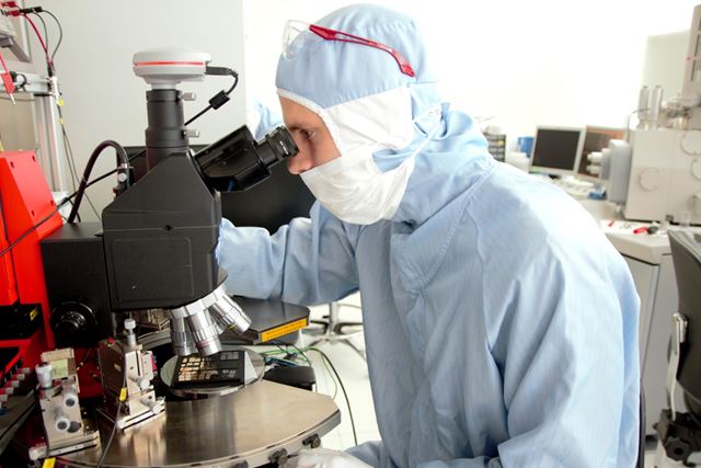
Jo Gjessing, seen here studying a wafer that will later be diced into MEMS chips. The wafers are made using a half-millimetre thick silicon wafer with a 100-nanometre platinum electrode coating. Photo: Lisbet Jære.
The piezoelectric ceramic film enables small microsystems to move rapidly with minimum energy consumption. The material also generates a voltage when it is put under strain, enabling it to be used as a sensor.
Multiple applications
Mechanical systems containing components that are well under half a millimetre in size may sound futuristic, but most of us are using this technology on a daily basis. For example, the Airbag sensor in your car is in fact a small MEMS accelerometer, and if you are travelling by air there is most probably a MEMS pressure sensor, manufactured here at SINTEF MiNaLab, in the altimeter and speedometer system.
About MEMS and microsystems:
Micro-electromechanical systems (MEMS) are miniaturised systems ranging in size from a few micrometres to a few millimetres that can perform both electrical and mechanical functions. The most common mechanical material is silicon and the manufacturing methods are the same as those used in production of microelectronics. Other materials such as ceramics, polymers and metals are incorporated to provide the systems with a variety of functions. Researchers and developers working with MEMS have produced a large number of microsensors for almost every application you can think of, such as for temperature, pressure, inertial forces, chemical substances, magnetic fields and radiation. There are also MEMS actuators that are used in small mechanical switches, small resonators used in biosensors, small pumps and valves used to control fluid flow during analysis, and small lenses and mirrors used to manipulate light, as described elsewhere in this article.
It is often the case that the lifetime of the microsystem version of a given component exceeds that of the macro-version. Source: SINTEF
“The main benefit of combining piezoelectric materials with MEMS, so that we get piezoMEMS, is that it opens up entirely new possibilities for designing new unique components that has perhaps not been possible to realize up to now.
“We’re seeing that piezoMEMS chips of this type can be enabling components in IoT (Internet of Things) applications, such as for smart homes, smart energy, smart mobility, etc., in which remote monitoring using new types of sensors is important. “We’re now developing several new MEMS chips directed at these markets”, says Tyholdt.
Improved plastic recycling
PiezoMEMS can be a key component in plastic recycling. Today, it is difficult to sort the various types of plastics during recycling. SINTEF has developed an optical sensor for the company Tomra which, among other things, is manufacturing reverse vending systems for drink container recycling, that can separate different types of plastics.
“This technology is very interesting to us”, says Geir Sæther, Director of Technology at Tomra. “We currently operate with another technology that is getting the job done. But, it looks as though the technology we’ve developed with SINTEF can do the job both better and at a lower cost”, he says.
The method used is spectroscopy. The PiezoMEMS chip is an adjustable optical filter that analyses near infra-red light that has either passed through or been reflected by the plastic. Different plastics carry different infra-red fingerprints, depending on which light wavelengths that pass through or are reflected, and these are measured by the optical filter. In this way it is possible to distinguish the different types of plastics so they can be sorted and recycled correctly.
Whether or not Tomra will advance this technology depends on developments in the deposit bottle market.
“The technology works very well for this purpose”, says Sæther. “We will also be looking into whether it can be used for the recycling of other products”, he says.
“One possibility might be its application at waste disposal stations that sort the different types directly”, adds Tyholdt. “This may mean that more of the plastic we use can be recycled. This will be cheaper because there will be less need for expensive cleaning processes”, he says.
Faster than lightning
Tyholdt relates how the company Polewall uses piezoMEMS technology in a product that may revolutionise the roll-out of high-speed internet systems and the 5G network. The technology is highly suitable in densely built-up areas where it is difficult to lay cables and where there is interference between WiFi signals.
“The answer is to transmit information using laser light, in the same way as in fibre optics, except without the fibre”, says Tyholdt. “The trick is to hit and then hold the laser on a small target point 200 metres away. This is something of a challenge, and this is where the MEMS chip comes in, acting as a mirror measuring 3 x 3 millimetres. Because it responds so quickly, the mirror can correct the laser beam so that it always hits the distant receiver, even if a tower block is swaying in the wind and there are people about”, he says.
Detecting gas leaks and contaminated water
Tunable Infrared Technologies is a start-up company spun-off from the SINTEF MiNaLab. It employs a method similar to the Tomra approach, but this time for detecting gases instead of plastics.
“Right now, we’re conducting a project to quantify water quality in fish farms by measuring the CO2 concentration in the water”, says Thor Bakke, who co-founded the company in 2015.
The approach is the same as that used to separate different types of plastic and here too, the MEMS chip is an adjustable optical filter. The gas has an infra-red fingerprint that is detected and measured by the optical filter. It is possible to program the filter so that it can distinguish different gases and measure their respective concentrations. In contrast, a standard gas sensor can normally only detect one specific gas mixture.
“Another project we’re running focuses on monitoring of transformers”, says Bakke. “The fact that some transformers start to burn is a problem. Today’s sensors are unreliable and can set off false alarms, or no alarms at all, even when they should. Using this technology, we can detect anomalies in the gas concentration. Several energy companies have shown interest”, he says.
Market launch
Tyholdt says that it has taken some time to generate interest in the technology as a commercial proposition, although this is not unusual for new products manufactured using new processes. The technology and camera lens design for the company poLight was already in place in 2006, but no process existed for mass production of the product. But now the company is ready to introduce its product to the market.
“The current trend towards digitalisation of the society means that we’re encountering increasing interest in piezoMEMS technology from industry both in Norway and overseas”, says Tyholdt.