Sensor types
Contact person

Microstrip sensors
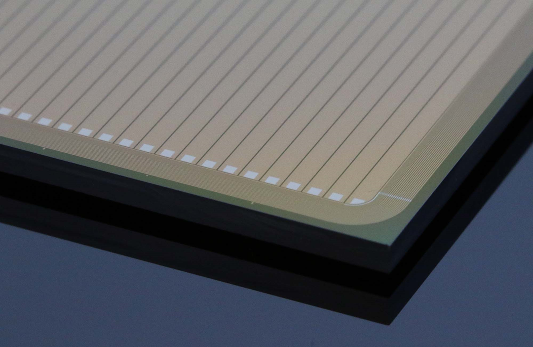
Microstrip sensors are used in applications where good position resolution and fast readout are important. A typical example is vertex detection in high energy physics collider experiments at international research laboratories such as CERN and Fermilab. Industrial applications include X-ray analysis and medical imaging. Our most popular strip sensors are P-on-N but N-on-P that can potentially provide a higher radiation tolerance is also available at SINTEF.
Single-sided strip sensors
Single-sided sensors have P+ implants formed as long strips on one side of the side. The window side has a highly doped uniform N+ implants and is usually covered by a layer of metal by choice.
Double-sided strip sensors
One side of a Double-sided sensors is like the strip side of a single-sided sensor with P+ implanted strips (P-side). On the opposite side, N+ implants (N-side) will be the long strips that are orthogonal to the strips on the P-side to provide two-dimensional position information. The N+ implanted strips on the N-side are isolated either by P-spray or P-stop or metal field plates biased to form an inversion layer between the strips. The isolation is needed isolate the strips that can be shorted due to the accumulation layer formed by the positive charge in the field oxide required on the silicon surface. The same approach is used for isolating strips and pixels for N-on-P technology.
Sensor Coupling
Microstrip sensors can be made DC coupled, or AC coupled. On DC coupled sensors, each strip connects directly to a metal pad for direct wire-bonding that will connect the strip to a single channel in an amplifier. In an AC coupled sensor, the sensors have integrated coupling capacitors and resistors-on-chip for signal readout and biasing, or alternatively, using a FOXFET structure. The FOXFET structure facilitates possible electrical testing, as the I-V characteristics of the sensor can be measured by making only two contacts: one to the P+ bias line on the P+ strip side and one to the N+ contact on the window side. The position resolution of a strip sensor depends on the center-to-center distance between the strips, called the pitch. By using charge division readout, the position resolution of the sensor can be pitch/√12.

Pixel sensors
A pixel sensor system has the advantage of offering very fast readout, without the position ambiguity of double-sided strip sensors when hit by several particles simultaneously. Each pixel is directly bonded to a channel in a Front-End ASICS using bump-bonding. The ASICS is then bonded face-to-face to the pixel side of a sensor. The key technological advantage of pixel sensors over double-sided strip sensors is that pixel sensors offer two-dimensional position resolution with a much-reduced fabrication cost and complexity.
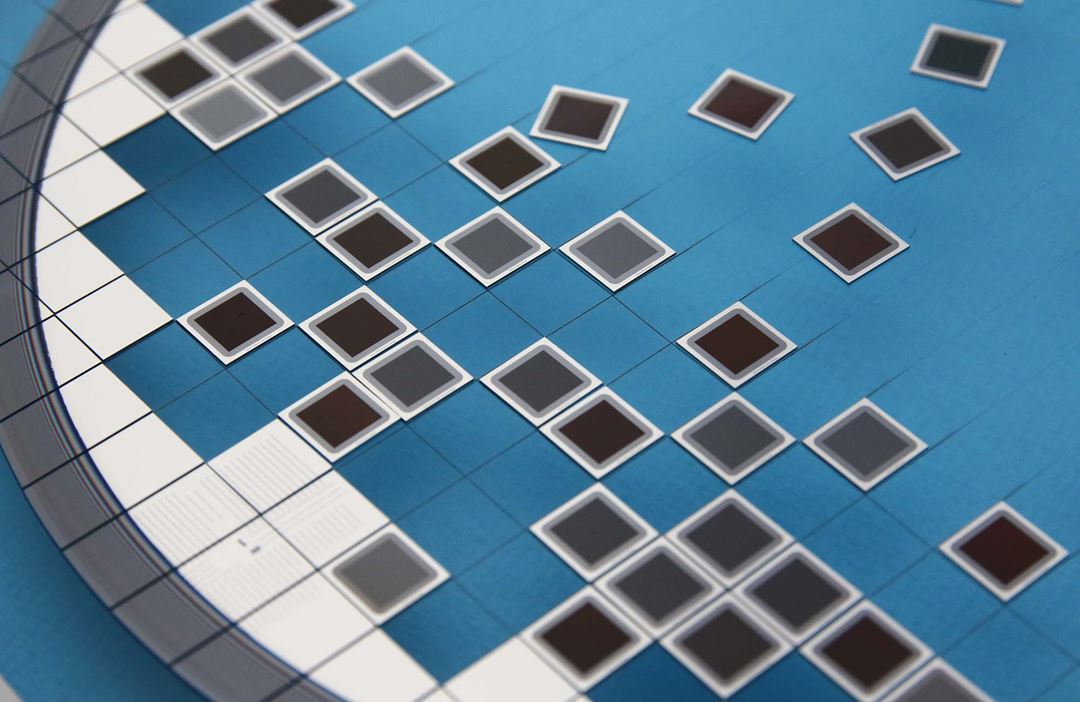
SINTEF can manufacture pixel sensors with element as small as 10 x 10 µm2 and a pitch of 25 µm, up to several hundred thousand pixels. The spatial resolution of flip-chip mounted sensors is limited by the area of each electronics channel. When coupled with a shallow entrance window, our pixel sensors are sensitive to a wide range of radiation energies and types including low energy particles and soft X-rays. Our standard sensor thickness ranges from 300 µm to 1 mm. When coupled with some minor, additional process modifications, we can also offer thin sensors (≥ 10 µm) and sensors that are 2 mm thick.

Silicon Drift Detectors (SDD)
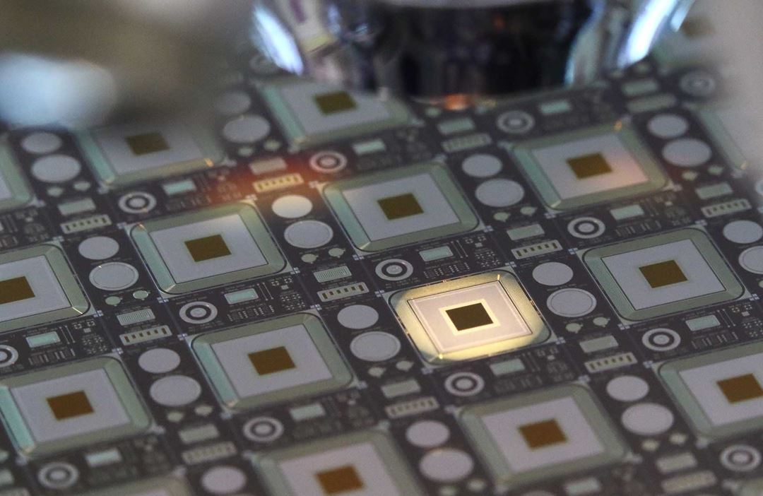
Silicon drift detectors have a cathode on one side that acts as an efficient entrance window for incoming radiation. On the other side of the detector, concentric cathode rings are used to set up a lateral electric drift field towards a small central anode. This configuration results in a sensor with extremely low capacitance for applications requiring very low noise levels and unsurpassed energy resolutions at low X-ray energies. SINTEF produces SDDs for different customers based on custom designed proprietary layouts and processes.
Photodiodes
Conventional PIN photodiodes
SINTEF can design and fabricate silicon PIN photodiodes tailored to customer requirements. The substrate material (active thickness, type, and resistivity), the actual design and process parameters can be chosen by our customer to meet your application needs. Examples of design and process parameters are:
- Isolation structures
- Edge termination structures
- Doping concentration and profiles
- Surface passivation
- Material and thicknesses of anti-reflective coating
These parameters will be chosen by you to meet your requirements of your device such as dark current, shunt resistance, breakdown voltage, spectral responsivity, time response, dynamic range, crosstalk, linearity, and radiation tolerance.
Photodiodes with active substrate down to a few µm thick can be manufactured using epitaxial (EPI) or Silicon-On-Insulator (SOI) wafers. Alternatively, the active area can be thinned down when using a silicon substrate by our in-house wet chemical etching of silicon to a desired thickness. Bulk wafers up to thickness of 2 mm can be used for enhanced NIR response. Doping processes that lead to extremely shallow p-n junctions can be implemented for significantly enhanced blue and UV responses. Our photodiodes can be used in a wide range of applications including material analysis and waste sorting, space, and medical imaging.
SINTEF is also carrying out R&D on avalanche-based silicon photodiodes and their monolithic integration with other photonics components such as waveguides and optical filters.
Induced-junction photodiodes
SINTEF has recently developed photodiodes based on induced junction technology in which the p-n junction is formed by the inversion of the silicon surface due to fixed charge in the passivating dielectric. These photodiodes exhibit record quantum efficiency at room temperature, and quantum deficiencies as low as ~1 ppm. Even though these photodiodes have been optimized for the 400-850 nm spectral range, they also have excellent UV-response. R&D is ongoing to extend the application of these photodiodes to the UV range (down to 200 nm) by improving their UV-radiation hardness without sacrificing their excellent sensitivity.
The induced junction photodiode has been developed primarily for applications that require measurement of optical power with very high accuracy such as photometry and radiometry. However, many other applications can benefit from the exceptional performance of these photodiodes.

Low Gain Avalanche Diodes (LGAD)
We are also developing Low Gain Avalanche Diode (LGAD) for low energy X-ray photons in collaboration with various synchrotron facilities in Europe and the USA.
3D & Edgeless Detectors
SINTEF is the second laboratory in the world to realize full 3D sensors with edgeless periphery after Stanford Nanofabrication Facilities. Through substrate, vertical electrodes are realized by DRIE technology. In the first SINTEF full 3D design, the electrodes are filled with highly doped polycrystalline silicon. These sensors are currently offered to high energy physics experiments to tolerate the stringent radiation hardness requirements. The geometry of through-substrate electrodes offers advantages such as ultra-high radiation hardness and ultra-fast time response.
Edgeless detectors
An edgeless detector has the entire periphery surrounded by a through substrate electrode that replaces conventional guard-rings for electric field regulation and isolation of defects caused by dicing of the sensor edge. The guard-rings are a dead area insensitive to radiation for the sensor. Edgeless detectors allow tiling without dead areas in large imaging system. When serve as an edge-on detector for low energy photons where the sensor is illuminated on the edge, offering high efficiency at a wide range of photon energies. Today, we offer edgeless detectors up to 300 µm.
3D silicon-based detectors for neutron imaging
With a suitable neutron converter, silicon-based neutron detector offers superior spatial resolution, bringing a major step forward in neutron imaging. Using conventional planar technology, the neutron detection efficiency in silicon-based detector is rather low. Our micro-structure technology when implemented for neutron detection provides a significant improvement in detection efficiency. We are currently in collaboration with several institutes and universities including the European Spallation Source to develop the next generation silicon detectors for neutron imaging.
3D Microdosimetry
In collaboration with the Centre of Medical Radiation Physics at the University of Wollongong, Australia, a pioneer in solid state microdosimetry, SINTEF has developed a state-of-the-art sensor technology for Quality Assurance and Treatment Planning in modern particle therapy that requires extreme precision in monitoring for patients' safety. The main breakthrough at SINTEF is the development of silicon-based microdosimeter that mimic the radiation effects in tiny volumes, just like measuring the radiation effects accurately in biological cells. The technology has been made feasible using micromachining and advanced in-house sensor technology. The collaboration has published numerous journal articles on the developed sensors and is currently working towards a commercially viable solution for particle therapy centres around the world.
