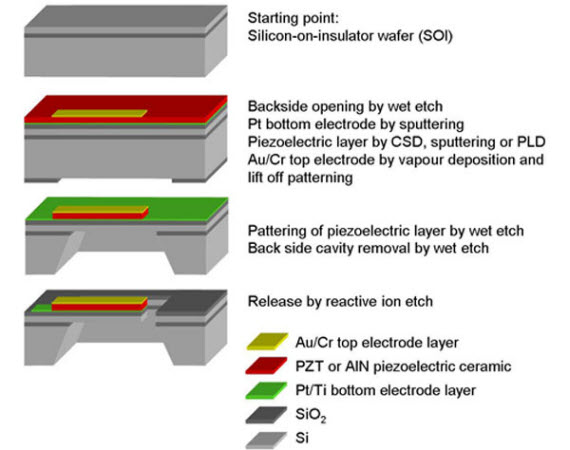
The MEMS-pie project:
Piezoelectric microsystems from the laboratory to production


  Sixth Framework Programme


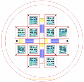
Test wafer production01
Test production
Qualified procedures are developed through processing and analysis of test wafers. The test wafer design contains more than 500 device elements of sizes between 10 µm and 1 mm. The device elements are cantilevers, plates, bridges and fixed membranes.
     
Design overview of the test wafer developed by the project. Twelve 15x15 mm squares contain a large number of basic design elements. Eight rectangles are dedicated to four-point bending tests to be performed after dicing of the wafer.  
 

Piezoelectric MEMS devices are produced through a series of deposition and etching steps.

Automated poling and testing
A system for automated poling and testing of the devices at wafer level has been developed. The wafer is mounted on a programmable xyz-table with a heating chuck. The devices are addressed sequentially and can be poled and tested individually at up to 160 °C. C(V) and I(V) measurements are routinely carried out and the system is to be integrated with an aixACCT TF2000 ferroelectric analyzer that will enable automatic measurements, including:

  • ferroelectric hysteresis, 
  • fatigue behaviour,
  • impedance sweeps (for electromechanical characterisation including determination of mechanical resonances).
   
Photograph of mounted cantilever elements after processingAutomated probe station for automatic poling and mapping of device performance across a wafer. 

Published October 26, 2006

These web pages do not represent the opinion of the European Community and the Community is not responsible for any use that might be made of data appearing in them.