The MEMS-pie project:
Piezoelectric microsystems from the laboratory to production


  Sixth Framework Programme


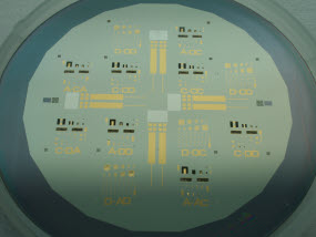
Piezoelectric thin films for new MEMS devices

Many companies have innovative ideas for new types of sensors and actuators that are based on silicon technology with integrated piezoelectric functional elements. Reliable technology for production of such systems is a key tool to realise the new products. The aim of the MEMS-pie project is to develop validated procedures for integration of piezoelectric thin films into micro-electromechanical systems (MEMS) on an industrial scale. Qualified production routes will form the basis for a new foundry service after completion of the project.


Test wafer (100 mm diameter) after processing. The wafer contains more than 500 piezoelectric test devices.  


Powerful actuation and efficient sensing


Piezoelectric materials have a unique ability to transform electrical energy directly to mechanical motion, or the opposite: transform movements or vibrations to electrical signals. They are used in various electrical and acoustical equipment, like ultrasonic scanners, hydrophones, microphones, loudspeakers, accelerometers, gyros, ink-jet printers, positioning systems, pressure sensors and for energy harvesting. The main drive to develop microsystems with this technology is based on a push from established industries that use piezoelectric thick film or bulk elements in their existing products and see a need for smaller devices with improved functionality and/or reduced energy consumption. MEMS developers have also expressed a desire for a technology that can deliver powerful and efficient actuation for the next generation of MEMS devices that will feature increased complexity and lower power consumption to allow for example mobile operation.


Based on the results from the MEMS-pie project, the partners are able to offer assistance in all the phases required to realise new piezo-MEMS devices;

• Concept evaluation
• Modelling and design
• Assessment of processing routes
• Wafer-level processing in clean-room
• Wafer-level testing and verification

Project e-room (members only)

Henrik Raeder
Research Manager, SINTEF
MEMS-pie Coordinator
Phone: +47 977 14 975
E-mail:

These web pages do not represent the opinion of the European Community and the Community is not responsible for any use that might be made of data appearing in them.