Non-standardized processes can be combined with standard Si/glass and polymer processes for enhanced functionality. The combined technologies often involve materials not used in the standard processes. Such mixing of the available microBUILDER technologies allows for improved functionality and higher performance of a variety of new devices. The processes offered through microBUILDER are technologies that enhance the functionality of separate silicon chips or separate polymer chips, or they are possible to combine with both silicon and polymer chips.
Technologies that increase the functionality of silicon chips:
Technologies and elements that increase the functionality of polymer chips:
Technologies that can be used in combination with both silicon chips and polymer chips for increased functionality:
Deep Reactive Ion Etch SensoNor/SINTEFThe maximum depth of RIE silicon channels processed by the standard SensoNor MultiMEMS MPW is limited to 10 µm. For most microfluidic applications these channels are too shallow. Glass channels offered by the MultiMEMS MPW are deeper, but the depth is fixed to 310 ± 15 µm. Moreover the glass channels are always rounded and have a substantial amount of under-etch and a high etch depth tolerance, and the applications are therefore limited. The new DRIE add-on process offered by SINTEF / SensoNor offers flexibility of channel depths. The standard depth is 100 µm, but shallower and deeper channel depths can be offered. DRIE silicon channels can be made with an aspect ratio up to 1:15. Benefits of silicon channels compared to glass or polymer channels are precisely defined dimensions with sharp corners. Sharp corners are important for several applications, e.g. for valves and for cell lysis (to dissolve the cell membrane). The DRIE process is optimized to obtain smooth surfaces which are highly important for microfluidic applications.
DRIE combined with the MultiMEMS manufacturing was used for the first microBUILDER demonstrator.
Standardized read-out electronics for piezoresistive sensors HSG-IMITPiezoresistive electro-mechanical transduction is widely used in micro-machined sensor elements. In such elements changes in mechanical stress can be detected as a change in resistivity. The change in resistivity is therefore directly related to changes in the parameter which is to be measured, e.g. pressure. A Wheatstone bridge configuration with four resistors is widely used, utilizing the high gauge factor of the silicon resistors. The SensoNor MultiMEMS MPW process offers buried conductors, piezoresistors, thin silicon diaphragms and cantilevers, elements which are typical in several types of piezoresistive sensors. Standardized read-out electronics for such sensors provides an easy-to-use interface for the customer. The microBUILDER read-out electronics can be used for temperature compensation, calibration, linearization and amplification of the voltage signal from the inherent Wheatstone bridge. The amplification factor can be easily adapted to different sensor designs.
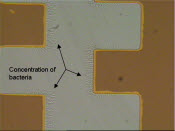
Gold patterning on silicon and glass SINTEFGold patterns on surfaces are combined with microfluidics in a wide variety of applications, both for commercial use and for research devices. Gold patterns on flat surfaces can be used for positioning and immobilization of cells, e.g. fruit-fly embryo. In sample preparation and particle / cell concentration chips, fine structured electrodes are used for di-electrophoresis (DEP) where e.g. bacterial cells can be retained. If the gold electrodes are patterned on a glass wafer, the glass wafer can later be bonded to a silicon wafer with channels, cavities and integrated sensors. The rare cells / bacteria can then be concentrated at the gold electrodes, while the rest of the sample is flushed away. Cell preparation and bio assay can then be carried out in the shared silicon / glass / gold system. Gold electrodes can be used for electrical field generation in electro-osmotic pumps, in electrochemical sensors or as heaters. Gold surfaces are also used for surface plasmon resonance (SPR) detection of specific binding reactions. Gold patterns are often used as binding areas for thiol self-assembled monolayers, onto which specific molecules for biochemical assays can be attached.
The gold patterning process on silicon can be further developed to yield freestanding structures, e.g. cantilevers and membranes, with gold on top. Thiol and / or bio functional layers can later be added and the structures can then be used as mechanical biosensors. Complementary antibodies or DNA strands can bind to the attached receptor molecules and the molecular binding can be monitored by external, optical detection (color, fluorescence or beam bending) or by piezoresistive sensing as an integrated part of the sensor.
Piezoelectric filmsMicroBUILDER offers two different technologies for piezoelectric films; theMoveMEMS thin film PZT process and the Tronics thick film PZT process. The two processes are different in the manufacturing approach with respect to the piezoelectric film thickness and quality and thus the resulting actuation/sensing voltages and the mechanical forces. The application areas are therefore different. Please consult the microBUILDER partners for choosing the best technology for your application.
Some of the key differences between SINTEF and Tronics PZT processes are summarized below:
MoveMEMS thin PZT (SINTEF)
Thick PZT (TRONICS)
Displacement / Force
Low
High
Drive voltage
Key feature
Integrated deposition process on flat surface
Adhesive bonding within cavity
MoveMEMS PZT - Piezoelectric thin film SINTEFThe reliable integration of piezoelectric thin films into MEMS is a key enabling technology for a wide range of future products. Examples include ultrasonic imaging transducers, pressure and flow sensors, accelerometers, acoustic wave devices, energy converters, micro-motors, micro-pumps, and micro-sensors for chemical analysis. Piezoelectric materials allow energy conversion between the electrical and mechanical domain. Several sensor structures utilize both the direct effect (conversion from the mechanical to the electrical domain) and the converse effect (conversion from the electrical to mechanical domain (i.e. actuation)).
Applications can be classified according to those employing:
Direct effect:
Sensors, energy conversion
(AC coupled)
Converse effect:
Linear Actuators
Converse effect with
Resonant ultrasound excitation
Both effects in resonance:
resonant transducer
· Vibration sensor
· (accelerometer)
· microphone
· acoustic sensors
· energy scavenging from vibrations
· Optical scanner
· Optical switch
· Micro, nano probe
· Switch – Relay, RF switch
· Valve
· Droplet ejector, inkjet
· Ultrasonic stator for micromotor
· Liquid delivery
· Thickness Bulk waves: ultrasonic imaging (thick films), RF filters (thin films), transformers
· Ultrasonic waves in pMUTs: ultrasonic imaging, proximity sensors
Active damping
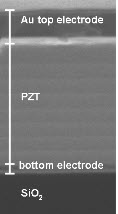
Several material systems of piezoelectric materials exist. The two most interesting alternatives for MEMS applications are aluminium nitride (AlN) and lead-zirkonium-titanate (PbZrTiO, shortened to PZT). Deposition of AlN is easy to industrialize, while the deposition techniques for PZT are far behind in maturity. However, PZT has an electromechanical coupling that is approximately 10 times higher than AIN and SINTEF has therefore developed the MoveMEMS PZT Chemical Solution Deposition (CSD) process.
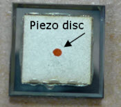
Piezoelectric thick film PZT Tronics
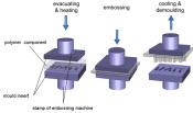
Within the framework of microBUILDER thick piezoelectric material is used as an actuator where electrical voltage is transformed into mechanical deformation. A piezoelectric disk glued onto a thin silicon diaphragm has been used as a micropump. A voltage applied to the piezoelectric actuator causes the silicon diaphragm to bow away from the pump chamber beneath and fluid will be drawn into the chamber. The pump-rate of a piezoelectric micro-pump can easily be changed by altering the actuation frequency.
Test assembly for microvalves TronicsmicroBUILDER has developed a microfluidic interface polymer slide for integration of silicon based sensors and microfluidic polymer slides into the thinXXS microfluidic construction kit/prototyping platform. An alternative solution for testing silicon microvalves manufactured by the microBUILDER partner Tronics, with placement and dimensions of inlet/outlet ports different from the microBUILDER standard, has been developed. This alternative solution makes possible testing of microfluidic features of a silicon die before shipment to customers.
Hot embossing HSG-IMITThrough the injection molding process offered by thinXXS, the microBUILDER customer has access to a low cost state-of-the-art technology for micro moulding of medium to high volumes of polymer devices. However, since design and fabrication of the needed molding tool is relatively time consuming and expensive, injection molding is not ideal for prototyping or for production of a smaller number of pieces.
The hot embossing technology developed at HSG-IMIT is a technology which ideally meets the needs for prototyping, as it is less expensive for smaller volumes and offers more flexibility with respect to the outer dimensions of the polymer components. Furthermore, hot embossing is compatible with mass production processes.
The hot embossing process is established for various substrate formats, e.g. rectangular standard microscope slide or CD-format disk, and for a selection of materials, e.g. COC, COP or PS.
Biocompatible Sealing of Polymer Chips HSG-IMITMicrofluidic devices usually have to be covered, e.g. to realise closed channel or camber structures. The sealing process offered through the microBUILDER partners HSG-IMIT and thinXXS is an indispensable technology for the leak-tight closing of such microfluidic structures. The sealing process needs to be biocompatible in order not to destroy any reagents or enzymes stored in the microfluidic structures ahead of the sealing process.
The offered standard sealing method is a Solvent Diffusion Bonding process. This process is chosen as standard because it offers very high bond strength with high fluidic tightness (i.e. no leakage). The sealed microfluidic devices have a very high optical quality. Moreover, the covering foil is applicable for temperatures up to 100 °C. No adhesive or intermediate layers are necessary and as so the Solvent Diffusion Bonding process is a simple procedure. The biocompatibility of the process is examined by the activity of a stored enzyme (alkaline phosphatese) before and after the sealing processes.
Other sealing processes as thermal diffusion bonding or sealing with a self adhesive foil are available on request.
Reagent storage HSG-IMITThe storage of reagents is a key feature for lab-on-a-chip systems in medical technology and the life sciences. It enables devices to be ready-to-use and only the sample has to be added to perform the system’s assay. As many assay systems tend to become mobile and partially disposable, methods to store reagents on the disposable part are of great importance.
In general, reagents can be stored both in liquid and solid state. While liquid storage is a milder procedure for less stable reagents, solid storage is suitable for long term storage. There can be no general approach to reagent storage as each reagent has specific requirements. Enzymes, however, are interesting reagents for dry storage as they are included in nearly all biochemical assays. They are a key component in various detection systems based on immunology, e.g. ELISA, PCR, and NASBA techniques. The amount of enzyme for an assay is relatively small, which allows for storage directly within the system’s fluidic network. Technology for dry storage of enzymes is therefore available through the microBUILDER consortium.
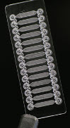
Filter slide thinXXSFiltering is an important sample preparation task in many microfluidic applications. Examples are DNA extraction for subsequent PCR and DNA micro-arrays, removal of particles according to size, and removal of solid debris from liquids. Plasma separation from whole blood is another example of a highly relevant sample preparation task in the development of point of care diagnostic devices.
Different separation membranes can be integrated in a standard filtering slide.
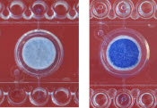
Cuvette polymer module thinXXSCommon to all lab-on-a-chip devices is the necessity to detect or observe the sample and measure parameters of interest. Many types of sensors exist to perform such analyses; however, it stands that optical analysis and sample observations are the diagnostic standard due to the extensive use of fluorescence detection techniques and other visual indicators.
The cuvette slide is intended to provide a visualization platform for biological samples that is consistent with the slides existing in the thinXXS microfluidic construction kit (modular testing system). The slide consists of multiple, individual viewing chambers which are connected to separate fluidic ports via inlet and outlet channels. The sample is therefore pumped into the chamber, where it can be combined with additional chemistry and observed by either an automated imaging system or by a microscope. Also, standard glass cover slips and microscope slides are used to seal the chambers and would allow the user to perform tests with custom treated glass slides or microarrays.
The self-assembly concept of the cuvette polymer module means it can be used in a wide variety of applications since the user has the flexibility to implement its own chemistry or materials. This includes many of the applications that are currently performed using microplates, cuvettes, and microscope slides. In particular, any processes which require interaction between a stationary or moving fluid and a biological material in an optically accessible cavity with a well-defined volume.
Hydrophobic patterning HSG-IMITValves and metering structures are core parts in medical and biotechnological devices used for diagnostics and/or for dosing. Valve structures able to stop and release flows are needed to e.g. ensure that reagents are dosed at the right time. Defined volumes of sample and reagents are a prerequisite to get analytical results. In microfluidic elements such valves and metering structures can be realized by hydrophobic patterns.
Hydrophobic patterns (patches) in microfluidic structures are areas with water repellent behaviour due to hydrophobic coatings (contact angle > 90°). In such areas the capillary movement of a liquid can be manipulated. Micro channels with hydrophobic patches can act as passive valves or for metering since self-priming by capillary force is stopped and an additional pressure is needed to re-establish the flow over the patched area.
Precise volume and position spotting of fluoropolymer-based solutions e.g. TEFLON AF is offered. The hydrophobic patches can be applied to surfaces after hydrophilization with e.g. PETOX or PEG.
Coatings for anti-binding or specific binding of bio macro-molecules on polymer and silicon chips and gold patterns on silicon or glass SINTEFSINTEF is offering a variety of well documented coating and chemical coupling procedures for modification of the surface materials as most frequently used in microsystems. These include the modification of polymeric materials such as COC (cyclic olefin copolymer) and typical silicon based chip materials such as silicon dioxide, glass and gold. For these materials SINTEF supply chemistries that may either to be used for chemical coupling of biospecific macromolecules such as proteins (e.g. antibodies, streptavidin or enzymes) and nucleic acid strands (DNA / RNA) or be used for establishing coatings that will minimize unspecific binding.
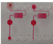
PDMS Channels in Polymer BMEThe microBUILDER partner BME-ETT has developed a laser manufacturing process for the realization of microfluidic channels in poly(dimethylsiloxane) PDMS. The offered laser processing technology is convenient for fast prototyping of PDMS microfluidic channel structures. The advantage of using PDMS as base material for fluidic structures is that sealing to any smooth surface can be realized by pressing the PDMS and the glass or silicon substrate together with relatively low force. The inlet and outlet connection, thus the micro-macro interfaces, can also be realized without additional sealing gaskets.
Published March 29, 2007
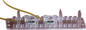
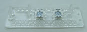
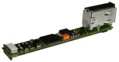
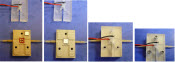
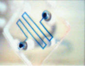
Interface slide for combining polymer and silicon technology
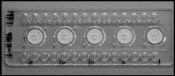
The interface slide with two integrated silicon based flow sensors
Part of deeper microfluidic channel with sharp corners processed by DRIE
Standard electronics read-out mounted on the interface slideElectronics read-out with flexboard connector and firewire
Fruit-fly embryo on gold Gold electrodes for cell sorting / concentration by DEP
Wafer with moveMEMS thin-film PZT
SEM image of a multimorph PZT stack (FEI Company)
Microphone array made by MoveMEMS
Micro-acoustic gas sensor made by MoveMEMS
A thick piezo actuator glued on a thin silicon diaphragm
The micro valve chip sandwiched between top and bottom support
Schematic of the hot embossing process
Disassembled frame tool for hot embossing
Cross-section of a microfluidc chip sealed by solvent diffusion bonding
Reagent storage slide
Filer slide
Part of a filter slide with an integrated separation membrane
The fluidic elements of a cuvette slide
Patterned hydrophobic film
Illustration of an ideal hydrophilic coating of a sticky surface
Microfluidic channel structure in PDMS