Piezoelectric oxides
Piezoelectric oxides
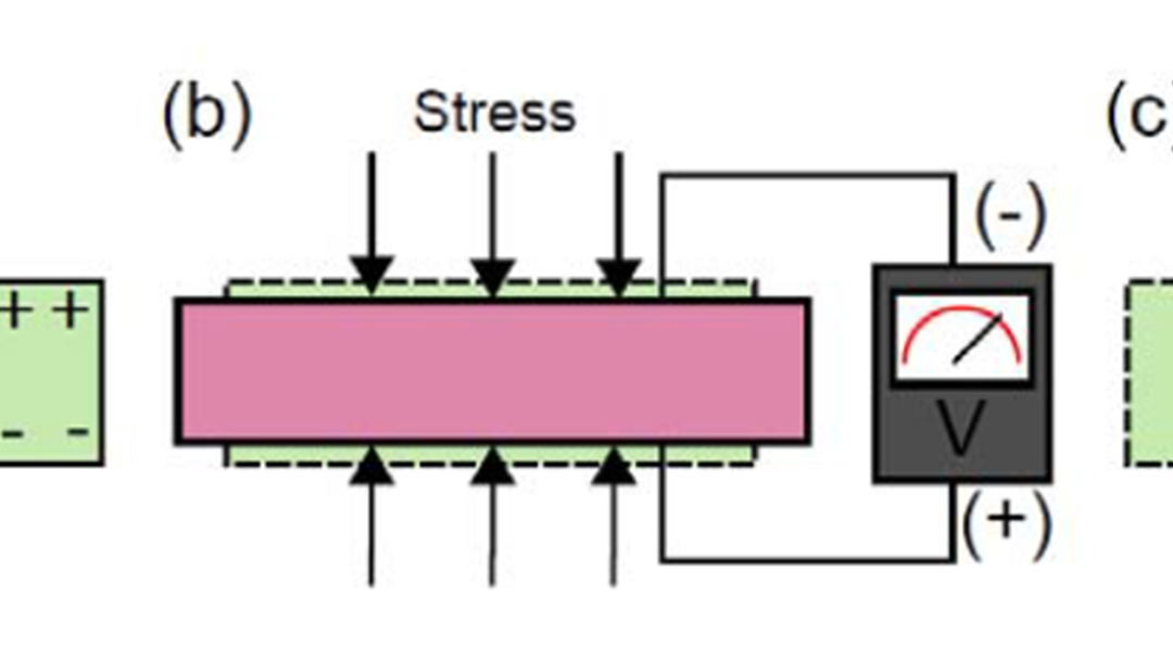
Piezoelectric ceramics are materials that generate electrical charge in response to applied mechanical stress, or vice versa. This coupling between electrical and mechanical signals makes them an enabling technology for a wide range of devices and products applied in various sectors of modern society. The applications range from widespread consumer products such as mobile phones and toys to sophisticated scientific instruments, such as actuators for atomic force microscopy.
Why lead-free?
In OXIPATH, we will focus on the development of lead-free piezoelectric oxides, to replace the current standard material PbZr1-xTixO3 (PZT) which contains hazardous lead. Making lead-free materials with comparable properties is especially important for medical devices, food-related applications, and disposable electronics.
BCZT thin films and nanofibres
One of the most promising lead-free piezoelectric materials is Ba0.85Ca0.15Zr0.10Ti0.90O3 (BCZT). Much research is devoted to optimizing the properties of KNN and related materials, mostly on bulk materials made by traditional powder-based ceramic methods. In Oxipath, SINTEF will prepare BCZT as thin films and as nanofibers.
High-temperature sputtering of BCZT
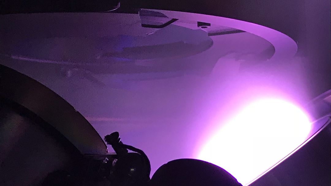
One of the objectives in Oxipath is to develop high temperature sputtering deposition procedures for BCZT thin films onto electroded Si wafers, with a piezoelectric coefficient d33 of at least 100 pm/V. SINTEF recently got a new Polyteknik Flextura deposition cluster system. The first lead-free piezoelectric thin films has been prepared and further optimization and characterization is on-going.
Piezoelectric nano-fibres
Some applications of piezoelectric oxides require larger-area and flexible devices, for instance for energy harvesting from wearable devices or anti-fouling membranes for water treatment. SINTEF will demonstrate such model devices using piezoelectric nanofibers produced by electrospinning. Fibres of BCZT has been prepared, and we are currently working on assembling the device and characterizing the output.
What SINTEF can offer
For more information about SINTEF's competence on piezoelectric materials and devices:
- Lead-free piezoelectric materials
- PiezoMEMS
For more information and other projects related to piezoelectric oxides:
- PiezoMed with our collaborators at NTNU


