Our working tools
Contact person

Processing facilities
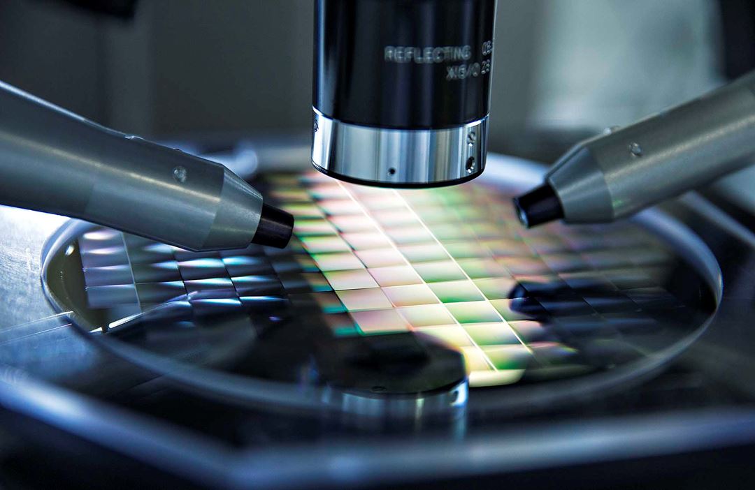
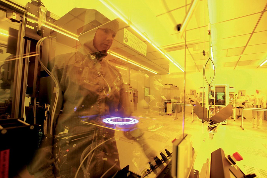
SINTEF MiNaLab fabrication facility contains a full processing line for 150 mm wafers. The line includes equipment for automatic photolithography, deposition and diffusion of dopants, thermal growth of silicon dioxide, LPCVD deposition of polycrystalline silicon and silicon nitride, PECVD deposition of silicon nitride and silicon dioxide, metal sputtering of Al, NiCr, Titanium and Au. In Micro-Electro-Mechanical-Systems technology, our facility consists of wet silicon etching, state-of-the-art tools for conventional and deep reactive ion etching (DRIE). The facility has a clean room area of 800 m2. While our standard wafer thickness is 300 µm, 500 µm and 1 mm, we also offer fabrication using wafers up to 2mm thick for applications that required improved efficiency at higher photon energy.

Design
The layout of photomasks and the design of sensors are done at SINTEF using a software, called L-Edit from Tanner EDA. The design files are checked and approved by our QA procedure before being sent to a mask supplier. Customers are welcome to carry out their own design and provide SINTEF with the design files.
Electrical Testing
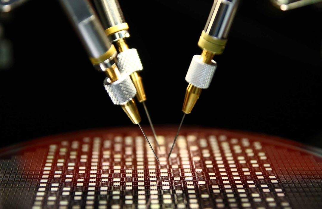
We have both fully automated and manual probe stations for electrical characterisation of sensors. The measurements are performed by Keithley and Agilent instruments. All wafer layout consists of several standard test structures from SINTEF that include a simple pad diode, MOS capacitor, gated diodes, and other features such as Kelvin structures. The qualification of each batch is done by measuring the test structures. We will tailor the qualification of other pixel and strip sensors to your needs.

Process & Device Simulation
Theoretical modelling is a vital tool for the development of technological processes and designs for achieving good yield and for optimization. Here we use the ATHENA and ATLAS providing by Silvaco Inc. ATHENA is the processing modelling while ATLAS is the device modelling.
Silicon Micromachining
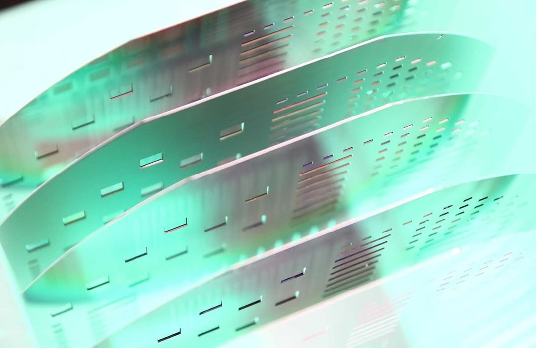
Using Micro-Electro-Mechanical-System technology at SINTEF, radiation sensors consist of 3-dimensional microstructures can be fabricated. The first established sensor technology using MEMS is our thin detectors, achieved by wet anisotropic etching of silicon. Using this anisotropic etch, sensors with active areas of ≥ 1 cm2 down to 10 µm thick with a ±1 µm thickness uniformity and other microstructures such as pyramidales structures can be produced.
In our more recent development, state-of-the-art Deep Reactive Ion Etching (DRIE) techniques offer the possibility to realize narrow holes and trenches with an aspect ratio as high as 60:1. This has been successfully implemented for the realization of through-silicon VIAS for vertical integration of sensors and readout electronics. In radiation sensors, DRIE has successfully prototyped radiation hard 3D detectors and edgeless sensors with zero dead periphery.

