Our strategy is:
To develop and combine various experimental and modeling methods to provide insight into a large variety of materials properties. We use this insight to solve problems for relevant industrial applications and address future materials challenges.
We answer questions like "Did my experiment work?", "Why does not the material I produced function?", or "What went wrong with my materials processing?" A crucial step towards resolving such issues is to determine what the material structure looks like and what it consists of. We utilize a range of microscopy, spectroscopy and spectrometry techniques.
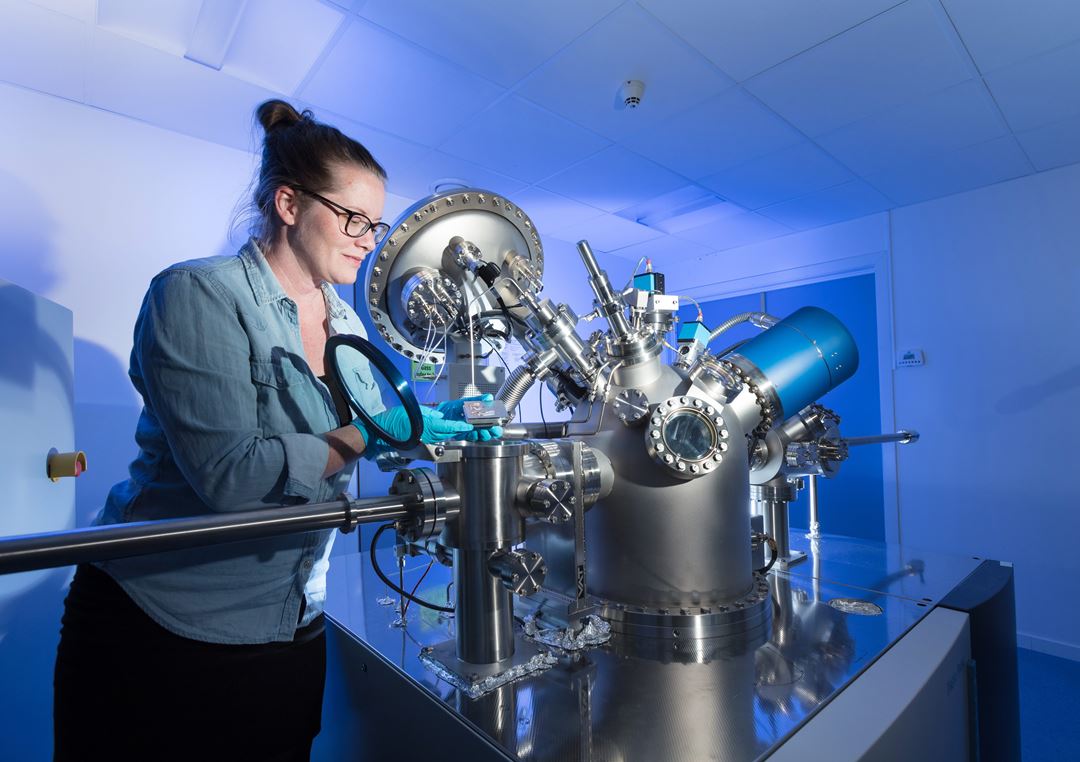
Using our microscopy facilities, we can image objects from the millimeter down to the atomic scale in great detail using optical and electron microscopes. The bulk and surface chemical composition of the specimen can be measured using electrons, x-rays, or ion based spectroscopy and spectrometry techniques. The surface topography can be measured and visualized using optical interferometry or atomic force microscopy.
If the interesting part is deep inside the specimen, a polished cross section can be prepared, allowing direct inspection of the interior of virtually any material.
We work with a wide range of materials including polymers, metals, ceramics, composite, hybrid materials and electronics components in bulk, particulate or thin film form.
Our targeted application areas for advanced materials characterisation include
- Metallurgical, process, chemical, construction, electronics industries
- Medical technology
- Energy technology
- Environmental technologies
- Catalysis
- Nanotechnology
- Oxidation, corrosion, bulk and surface material degradation
- Surface modification, surface film thickness measurements, thin and ultra-thin film technologies

