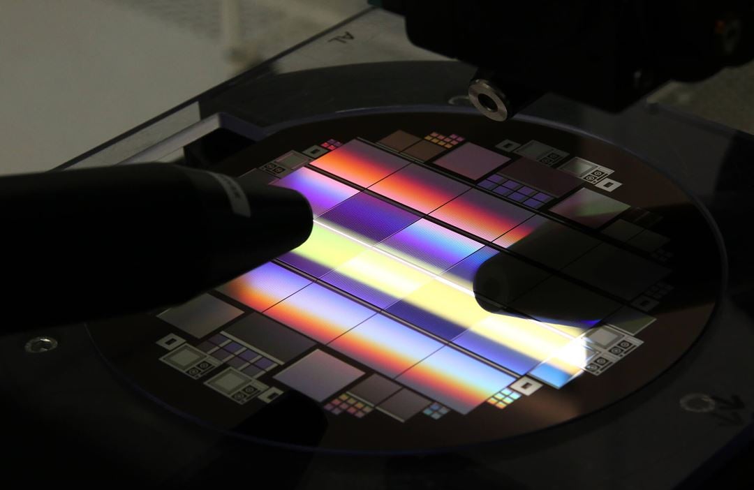
Our silicon radiation sensor technology
The silicon radiation sensor technology has evolved through a series of challenging projects and development programmes since the early 1980s. The fundamental fabrication technology and our long track record experiences enable us to design and deliver sensors that meet the most demanding requirements. Our cornerstone is our ultra-clean processing facilities in combination with a proprietary gettering process that achieves extremely low leakage current, down to 100 pA/cm2 for a 500 µm thick sensor in full depletion. In combination with appropriate design solutions, our sensor technology provides a component for ultra-low noise detection system. SINTEF MiNaLab has a complete Si processing line for 150mm wafers with state-of-the-art production equipment. Our lab is ISO 9001-2015, ISO 14001-2015, and OHSAS 18001:2007 certified.
OUR TECHNOLOGY OPTIONS
- P-on-N technology
- N-on-P & N-on-N technology
- Double-sided technology
- Double metal layers
- Biasing methods
- Shallow entrance window
Read more about our technology options.
Meeting your needs
Sensor design can be performed by SINTEF according to specifications and the needs of our customers. A fully completed design or even a full physical photolithography mask set can be provided by our customer. We pride ourselves for flexibility, and our openness in all discussions regarding your design, prototyping and manufacturing details, to tailor a product and service that meet your requirement in entirety.
OUR WORKING TOOLS
- Processing facilities
- Design
- Electrical Testing
- Process & Device Simulation
- Silicon Micromachining
Read more about our working tools.
Application areas and customers
Our radiation detectors are used for detection of optical photons, X-ray photons, high energy particles and heavy ions. Our sensors offer high spatial and energy resolution for X-ray imaging, material analysis, particle tracking, and ion identification and tracking. We provide services for a wide range of customers. These include international research organisations such as CERN, Fermilab, Stanford Linear Accelerator Centre, and Brookhaven National Lab, as well as industry and universities around the world. In addition, SINTEF provides prototyping, services, and products to industry, offering a wide range of radiation sensors and photodiodes for many companies worldwide, specialising in applications for material analysis, waste sorting and management, medical imaging, and optical sensing for space navigation.
Our products and sensors
SINTEF operates a 6-inch (150 mm) processing line. The standard silicon thickness is between 300 µm and 500 µm. However, SINTEF also offer sensors from 10 µm up to 2 mm thick. Thin sensors can operate in high dose environment while thicker sensors provide a much higher efficiency for higher energy photons. We have successfully demonstrated double-sided processing on 2 mm thick wafers, probably the first in the world. At present, we routinely manufacture strip and pixel sensors on 1 mm thick wafers.
SENSOR TYPES
- Microstrip sensors
- Pixel sensors
- Silicon Drift Detectors (SDD)
- Photodiodes
- Low Gain Avalanche Diode (LGAD)
- 3D & Edgeless Detectors
Read more about our sensor types.
Typical design and substrate specifications
SINTEF can design and fabricate silicon PIN photodiodes tailored to customer requirements. The substrate material (active thickness, type, and resistivity), the actual design and process parameters can be chosen by our customer to meet your application needs. Some typical parameters and specifications are:
- Wafer size: 150 mm
- Type: n-type or p-type
- Thickness: 300 µm – 1 mm
- Pitch: ≥20 um
- Resistivity:
- 1mm substrate: 10000 – 30000 Ω.cm
- 300 µm and 500 µm substrates: 5000 - 12000 Ω.cm
- Metal option: Aluminium ≥ 20 nm
- Entrance Window sensitivity ≥ 150 nm from sensor surface
